
The recent that researchers at Monash University have made a significant leap forward with a novel photonic technology. Published in the prestigious journal Nature Photonics, the work details what they claim is the first fully integrated, on-chip system that can generate, guide, and read information using the quantum property of electron “valleys”. This development, if scalable, could mark a pivotal moment for photonic technologies, promising fundamentally faster processing and lower energy use for AI and next-generation communications.
Table of Contents
A critical look at the claims reveals a familiar pattern in cutting-edge tech: a breakthrough in the lab that still faces a difficult path to commercial reality. The core innovation of this the technology is its ability to perform all necessary functions—generation, routing, and detection—on a single, compact device, a feat that has previously been a major bottleneck for the field. Moreover, the device operates at room temperature, a vital advantage over many quantum systems that require extreme and costly cooling.
Who Controls the Valley?
To grasp the importance of the Monash announcement, one must first understand the landscape of valleytronics. Unlike traditional electronics that use electron charge to represent data, valleytronics uses a quantum state known as the “valley degree of freedom”. This property, found in 2D materials like transition metal dichalcogenides (TMDs), allows information to be encoded in an electron’s momentum state, offering a path to computation with potentially lower energy loss from scattering. The primary advantage over its cousin, spintronics, is stability; valley states are not inherently tied to magnetic fields, which can be a source of instability.
The pursuit of a working this innovation is intense, involving research groups at institutions worldwide. The key challenge has always been integration. While scientists could generate valley-polarized light or detect it, doing both along with routing on one chip was elusive. The Monash team’s breakthrough was reportedly a novel stacking technique, allowing them to integrate ultra-thin TMD layers with engineered metasurfaces that manipulate light at the nanoscale. This overcomes the technical hurdles of growing these delicate materials directly onto photonic structures. Still, the field is rife with fundamental challenges, including short “valley lifetimes” where the quantum state quickly decays.
You might also like: Trillium ald system: The Critical Breakthrough for 2nm Chips?
Does the Monash Chip Live Up to the Hype?
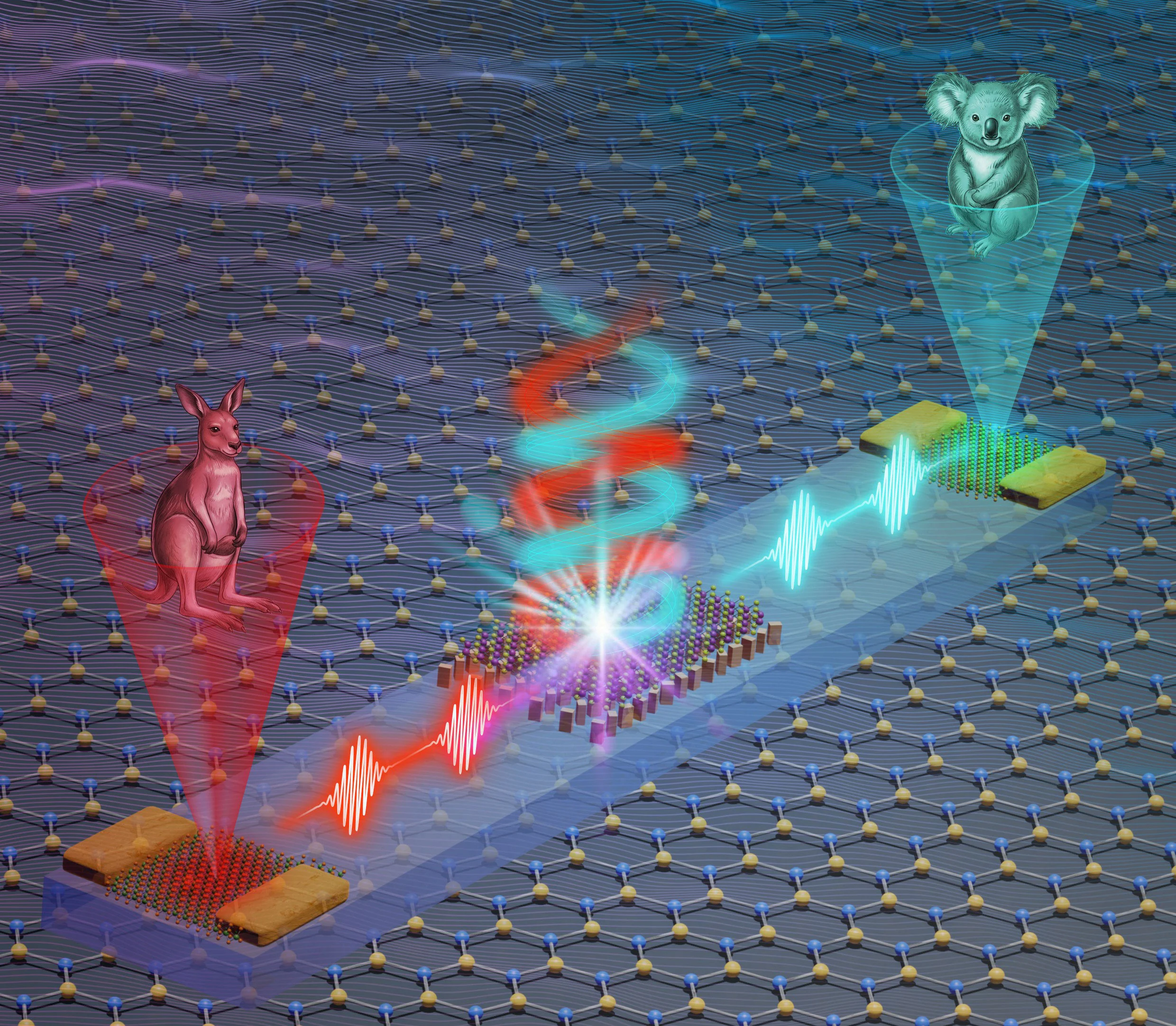
While Monash heralds a revolutionary the system, the published paper in Nature Photonics presents a more nuanced picture. The researchers successfully demonstrated the principle by encoding and processing two separate images simultaneously, a impressive proof-of-concept. This demonstrates the potential for managing multiple information streams. However, it is vital to distinguish between a laboratory demonstration and a scalable, manufacturable product.
The main point of contention revolves around scalability and material consistency. The “straightforward stacking approach” mentioned by the researchers is a manual, lab-based technique. Replicating this with the precision required for wafer-scale fabrication, the standard for the semiconductor industry, is a monumental challenge. Minor deviations in twist angle or strain in these 2D materials can drastically alter their electronic properties, making consistent production of a it an open question. The leap from a single successful device to millions of identical, reliable chips is where many quantum breakthroughs falter.
Friction Points for the photonic technology
The central challenge for the the platform lies in its materials. The very 2D materials that enable valleytronics, like MoS₂ or WSe₂, are also its Achilles’ heel. Achieving uniform, defect-free, large-area sheets of these materials is a well-known problem in materials science. An arXiv paper from March 2026, titled “Valleytronics in 2D Materials Roadmap,” highlights that scalable and reproducible control of these materials remains a primary obstacle.
Furthermore, even if the manufacturing challenges are solved, the “valley lifetime” problem persists. This refers to the timescale before an electron scatters and loses its valley information. In most materials, this lifetime is incredibly short, limiting the distance information can travel and the number of operations that can be performed. While the Monash the technology is a step forward in integration, it doesn’t fundamentally rewrite the physics of intervalley scattering that plagues all such devices. Until these fundamental material science and physics challenges are met, any commercial this innovation remains a distant prospect.
Recommended: Optical chip: A Critical Threat to Moore’s Law Has Emerpened
The Bottom Line on photonic technology
Ultimately, the Monash University breakthrough is a demonstrably significant academic achievement. It proves that a fully integrated, room-temperature the system is physically possible, solving a long-standing integration problem. However, the breathless hype surrounding it as the immediate future of computing is premature. The path from this successful lab demonstration to a commercially viable product is fraught with significant material science and manufacturing challenges that are far from being solved. This is a marathon, not a sprint.
Critical Signals to Watch:
* Watch for: Any announcements regarding successful wafer-scale fabrication of these integrated valleytronic devices, moving beyond single-chip lab results.
* A critical indicator: Research that reports a significant, order-of-magnitude increase in valley lifetime or diffusion length at room temperature.
* A key development: The first partnership between a university research group and a major semiconductor foundry like NVIDIA or TSMC to commercialize a photonic technology.
* Monitor: Progress in the “Valleytronics in 2D Materials Roadmap” that specifically addresses the challenges of scalability and valley depolarization.
As of May 2026, the photonic technology remains a tantalizing glimpse into a potential future for computing, but one that is still firmly rooted in the research lab.